Using X-rays, you can not only see the inside, but also see characters that disappeared from old documents 1,300 years ago or spy chips placed on the motherboard. However, recent X-ray technology enables reverse engineering by analyzing nanoscale IC chip structures.
Moore’s Law, which states that the number of transistors in semiconductor integrated circuits doubles every two years, is known to have come to an end. However, even if the speed drops, the CPU structure is still miniaturizing and densifying. Therefore, reverse engineering an IC chip requires tremendous effort and time, such as removing nanometer-level components one by one and imaging layered circuits using optical microscopes to electron microscopes. Also, since the IC chip is too small to be reassembled, valuable samples will be lost if reverse engineering is successful.
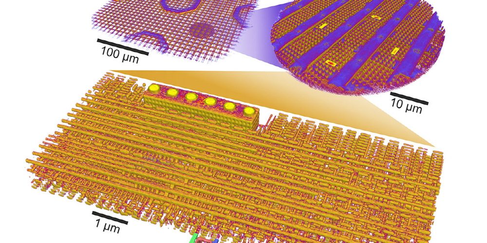
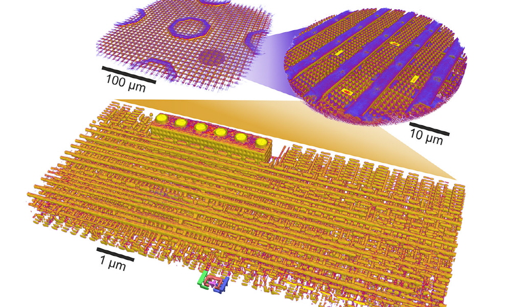
In the midst of this, a research team at the University of Zurich published a paper saying that it developed a new technology to analyze the structure of an IC chip using X-rays. It is said that using this new technology, called ptychographic X-ray laminography, can non-destructively reverse engineer X-rays irradiated by Synchrotron onto an IC chip.
The research team actually developed a similar technique in 2017, X-ray ptychography. However, due to technical limitations, it was not possible to clarify the detailed structure of the latest IC chip.
What bothered the research team was that if X-rays were irradiated directly onto the chip, they would absorb X-rays and could not obtain useful diffraction patterns. Therefore, the previously developed X-ray typography eliminated the method of estimating the IC chip structure from the appearance of scattering X-rays by irradiating X-rays at various angles using a 10-micrometer column.
On the other hand, the new technology solves the existing problem by irradiating X-rays at a diagonal of 61 degrees and balancing the accuracy and information lost by X-ray absorption. The IC chip inspection by the new technology first inspects an area with a side of 300 × 300 micrometers in a low resolution mode over 30 hours. And when the heart of the IC chip is found, this time, a 40-micrometer diameter region is analyzed for 60 hours in high resolution mode. Since X-rays have a photon-like nature rather than short-wavelength electromagnetic waves, a special camera called a photon counting camera is used, not the same lens used for observing visible light.
It is said that it has succeeded in identifying the structure of a 16nm node-sized chip circuit by creating a 3D model based on the obtained data.

Using this technology, it is possible not only to check whether the manufactured IC chip is structured as designed, but also reverse engineering of the IC chip with an unknown structure. The research team says that it takes 90 hours to diffract the IC chip now, but if the latest synchrotron such as Sweden’s Max IV Research Institute can irradiate sufficient flow rate X-rays, the inspection time could be shortened to less than an hour in the near future. In addition, it is said that it has already been criticized by the US national security authorities, and that it is considering use in security fields such as spy chip detection as well as industrial fields. Related information can be found here .


Add comment